Cache
Part of this section is from fabulous http://duartes.org/gustavo/blog/
Terms
- Cache Line
- L1 Cache
- L2 Cache
- FSB
- Agent
- request phase
- Memory type
- UC: uncacheable
- WC: write-combining
- WT: write-through
- WP: write-protected
- WB: write-back
- Cache coherence
- Memory mapping
When trying to understand complex systems, you can often learn a lot by stripping away abstractions and looking at their lowest levels. In that spirit we take a look at memory and I/O ports in their simplest and most fundamental level: the interface between the processor and bus. These details underlie higher level topics like thread synchronization and the need for the Core i7. Also, since I’m a programmer I ignore things EE people care about. Here’s our friend the Core 2 again:
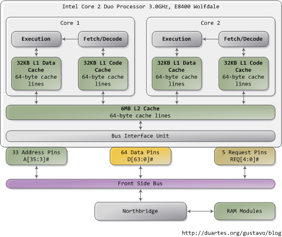 A Core 2 processor has 775 pins, about half of which only provide power and carry no data. Once you group the pins by functionality, the physical interface to the processor is surprisingly simple. The diagram shows the key pins involved in a memory or I/O port operation: address lines, data pins, and request pins. These operations take place in the context of a transaction on the front side bus. FSB transactions go through 5 phases: arbitration, request, snoop, response, and data. Throughout these phases, different roles are played by the components on the FSB, which are called agents. Normally the agents are all the processors plus the northbridge.
We only look at the request phase in this post, in which 2 packets are output by the request agent, who is usually a processor. Here are the juiciest bits of the first packet, output by the address and request pins:
 The address lines output the starting physical memory address for the transaction. We have 33 bits but they are interpreted as bits 35-3 of an address in which bits 2-0 are zero. Hence we have a 36-bit address, aligned to 8 bytes, for a total of 64GB addressable physical memory. This has been the case since the Pentium Pro. The request pins specify what type of transaction is being initiated; in I/O requests the address pins specify an I/O port rather than a memory address. After the first packet is output, the same pins transmit a second packet in the subsequent bus clock cycle:
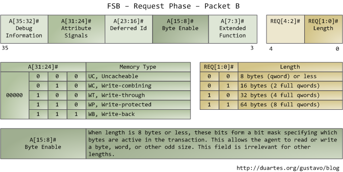 The attribute signals are interesting: they reflect the 5 types of memory caching behavior available in Intel processors. By putting this information on the FSB, the request agent lets other processors know how this transaction affects their caches, and how the memory controller (northbridge) should behave. The processor determines the type of a given memory region mainly by looking at page tables, which are maintained by the kernel.
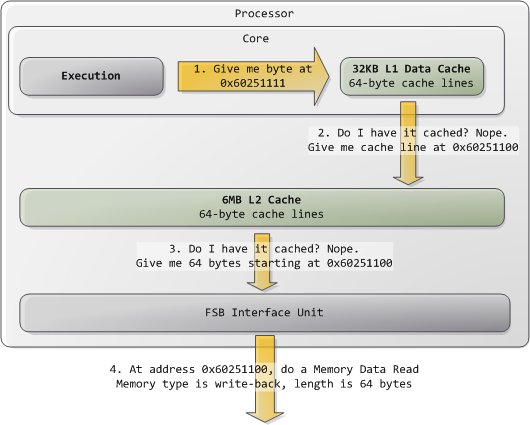
Typically kernels treat all RAM memory as write-back, which yields the best performance. In write-back mode the unit of memory access is the cache line, 64 bytes in the Core 2. If a program reads a single byte in memory, the processor loads the whole cache line that contains that byte into the L2 and L1 caches. When a program writes to memory, the processor only modifies the line in the cache, but does not update main memory. Later, when it becomes necessary to post the modified line to the bus, the whole cache line is written at once. So most requests have 11 in their length field, for 64 bytes. Here’s a read example in which the data is not in the caches:
 Some of the physical memory range in an Intel computer is mapped to devices like hard drives and network cards instead of actual RAM memory. This allows drivers to communicate with their devices by writing to and reading from memory. The kernel marks these memory regions as uncacheable in the page tables. Accesses to uncacheable memory regions are reproduced in the bus exactly as requested by a program or driver. Hence it’s possible to read or write single bytes, words, and so on. This is done via the byte enable mask in packet B above.
The primitives discussed here have many implications. For example:
Performance-sensitive applications should try to pack data that is accessed together into the same cache line. Once the cache line is loaded, further reads are much faster and extra RAM accesses are avoided. Any memory access that falls within a single cache line is guaranteed to be atomic (assuming write-back memory). Such an access is serviced by the processor’s L1 cache and the data is read or written all at once; it cannot be affected halfway by other processors or threads. In particular, 32-bit and 64-bit operations that don’t cross cache line boundaries are atomic. The front bus is shared by all agents, who must arbitrate for bus ownership before they can start a transaction. Moreover, all agents must listen to all transactions in order to maintain cache coherence. Thus bus contention becomes a severe problem as more cores and processors are added to Intel computers. The Core i7 solves this by having processors attached directly to memory and communicating in a point-to-point rather than broadcast fashion. These are the highlights of physical memory requests; the bus will surface again later in connection with locking, multi-threading, and cache coherence. The first time I saw FSB packet descriptions I had a huge “ahhh!” moment so I hope someone out there gets the same benefit. In the next post we’ll go back up the abstraction ladder to take a thorough look at virtual memory.
Write combine
What is write combining
WRITE COMBINING Once a memory region has been defined as having the WC memory type, accesses into the memory region will be subject to the architectural definition of WC:
WC is a weakly ordered memory type. System memory locations are not cached and coherency is not enforced by the processor’s bus coherency protocol. Speculative reads are allowed. Writes may be delayed and combined in the write combining buffer to reduce memory accesses..
What does this really mean? Writes to WC memory are not cached in the typical sense of the word cached. They are delayed in an internal buffer that is separate from the internal L1 and L2 caches. The buffer is not snooped and thus does not provide data coherency. The write buffering is done to allow software a small window of time to supply more modified data to the buffer while remaining as non-intrusive to software as possible. The size of the buffer is not defined in the architectural statement above. The Pentium Pro processor and Pentium II processor implement a 32 byte buffer. The size of this buffer was chosen by implementation convenience rather than by performance optimization. The buffer size optimization process may occur in a future generation of the P6 family processor and so software should not rely upon the current 32 byte WC buffer size or the existence of just a single concurrent buffer. The WC buffering of writes has another facet, data is also collapsed e.g. multiple writes to the same location will leave the last data written in the location and the other writes may be lost.
More Explanations
Most memory you deal with on a daily basis is cached; on CPUs, it’s usually write-back cached. While dealing with processor caches can be counter-intuitive, caching works well most of the time, and it’s mostly transparent to the programmer (and certainly the user). However, if we are to use the cache to service memory reads, we need to make sure to invalidate our cache entries if someone else writes to the corresponding memory locations. This is implemented using one of several mechanisms referred to as “coherency protocols”, which CPU cores use to synchronize their caches with each other.
Because while such mechanisms are in place for CPUs talking to each other, there is nothing equivalent for the CPU talking to other non-CPU devices, such as GPUs, storage or network devices. Generally, communication with such devices still happens via system memory (or by memory-mapping registers or device memory so they appear to be system memory, which doesn’t make much difference from the CPU core’s point of view), but the CPU is not going to be notified of changes in a timely fashion, so normal caching is out.
Originally, device memory used to be accessed completely without caching. That’s safe (or at least as safe as it’s going to get) but also slow, because each memory access gets turned into an individual bus transaction, which has considerable overhead. Now anything related to graphics tends to move a lot of data around. Before widespread hardware acceleration, it was mostly the CPU writing pixels to the frame buffer, but now there’s other graphics-related writes too.
So finally we get write combining, where the CPU treats reads as uncached but will buffer writes for a while in the hope of being able to combine multiple adjacent writes into a larger bus transaction. This is much faster.
Common implementations have much weaker memory ordering guarantees than most memory accesses, but that’s fine too; this kind of thing tends to be used mainly for bulk transfers, where you really don’t care in which order the bytes trickle into memory. All you really want is some mechanism to make sure that all the writes are done before you pull the trigger and launch a command buffer, display a frame, trigger a texture upload, whatever.